Smartphones, laptops and other electronic gadgets wouldn’t be possible without transistors—semiconductor parts similar to a light switch—that are comprised of thin films of some tens of layers of atoms or molecules. Smartphones require more than a billion transistors, and computers require even more.
Nicholas Strandwitz, the Harold Chambers Junior Professor in Materials Science and Engineering, specializes in a thin-film growth process called atomic layer deposition (ALD).
By fluctuating the temperature during the creation of films through thermally modulated ALD, Strandwitz is developing a new method of growing materials that could allow transistors to continue to shrink—and pave the way for the future of computing hardware.
Strandwitz’s project is supported by a CAREER Award from the National Science Foundation.
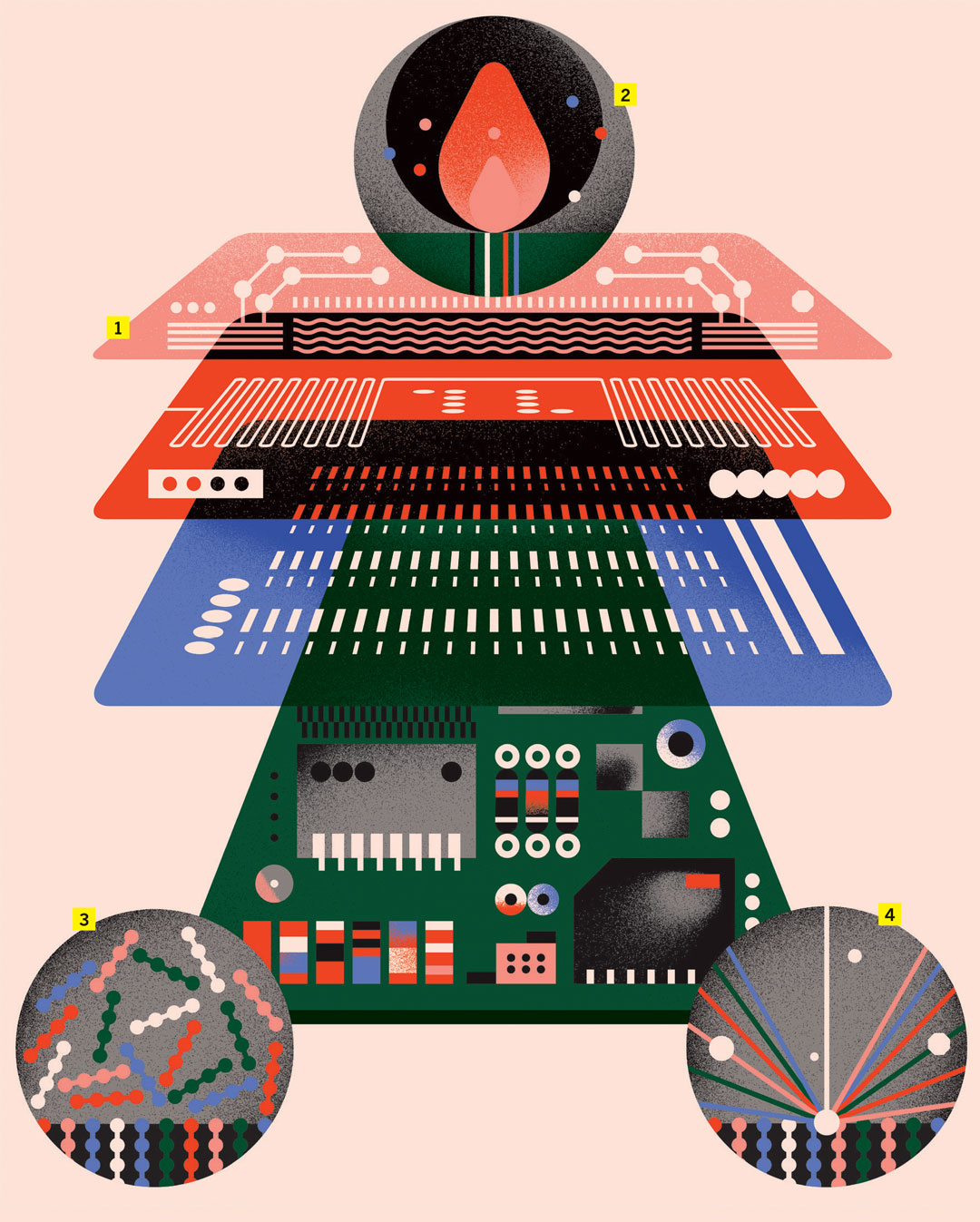
What the schematic shows:
- THIN FILMS. Transistors consist of films, parts of which are just 2.5 nanometers thick. The transistor itself is not much larger measuring at 10 nanometers and others even smaller.
- TEMPERATURE. Temperature is critical to the ALD process. It must be kept low enough—300 degrees Celsius and lower—so molecules don’t break apart on the surface of a silicon wafer and lead to a buildup of layers with the reaction no longer self-limiting.
- CRYSTALS. During conventional ALD, atoms arrange themselves into an amorphous, or “glassy,” state. Strandwitz wants to modify the process and gently add heat, allowing atoms to rearrange themselves into a crystal, or ordered array.
- MONITOR. Strandwitz envisions using reflected high energy electron diffraction, or RHEED, to measure the arrangement of atoms. An electron beam attached to a custom ALD system, placed at a very shallow angle and bounced off the surface, hits an electron capture screen, where it glows or lights up.
Story by Stephen Gross


