
The military advantage of radar equipment that can transmit further into the field is obvious. How to develop the new materials needed to achieve that goal is less so.
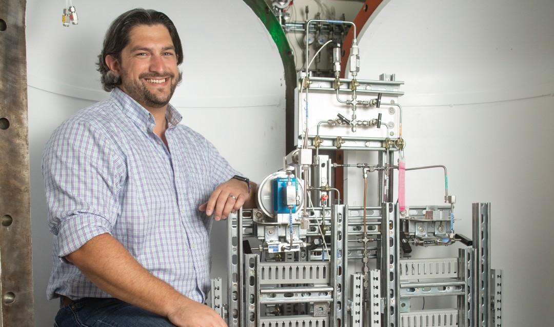
That’s the challenge Siddha Pimputkar, assistant professor of materials science and engineering at Lehigh, has accepted under a $1.1 million grant from the DEVCOM Army Research Laboratory.
“The Army is interested in radio frequency (RF) emitters, radar systems, that perform at higher power levels and frequencies to let them go farther into the field,” Pimputkar said. “To do that, you need better semiconductor materials.”
This military application is one example within a larger trend in materials science and engineering to develop semiconductors that have superior properties to the current state-of-the-art for specific applications.
Outgrowing Silicon
For decades, silicon has been the go-to semiconductor for use in electronics because of its abundance, availability at a very high crystal quality, and ability to be what scientists call “doped,” or having its electrical properties controlled through the introduction of impurities.
“Silicon works but it’s not ideal,” Pimputkar said. “We’re researching new synthesis pathways to make materials that have superior properties for the conversion of electricity at higher power.”
In more recent times, a new class of semiconductors has been developed that enable better performance for a variety of applications, including use at higher temperatures, handling higher frequencies and switching larger voltages. The two leading “wide-bandgap” (WBG) materials are gallium nitride (GaN) and silicon carbide (SiC).
The development of GaN was instrumental in the creation of blue light-emitting diodes (LED) for use in applications such as energy-efficient LED lighting. That advancement won a Nobel Prize for inventor Shuji Nakamura, under whom Pimputkar studied as a graduate student at the University of California, Santa Barbara.
This new class of materials is characterized by their wider bandgap, or the energy gap between the lower level at which an electron is non-conductive and the higher level at which it is activated as a conductor. The bandgap of these materials is approximately three times greater than that of silicon, offering greater energy efficiency and faster device speeds.
In addition to their use in current military radar systems, they have begun to gain wider adoption in applications such as 5G networks, electric cars and consumer electronics.
Staying on the Frontline
Much of the initial research that led to the development of WBG materials was funded by the Department of Defense and Department of Energy, which are compelled to remain on the forefront of new technology.
While WBG materials remain in relatively early stages of adoption, the military is already looking to benefit from materials with even higher capabilities. In 2020, the U.S. Army Combat Capabilities Development Command/Army Research Laboratory/U.S. Army Research Office (ARO) issued a call for proposals to develop ultra-wide bandgap (UWBG) RF electronics.
Ultra-wide bandgap materials have bandgaps greater than GaN’s 3.4 electron volts. Members of this class include diamond, aluminum gallium nitride (Al1-xGaxN), and beta-phase gallium oxide (β-Ga2O3).
“The challenge now is, can we do even better than GaN and SiC?” Pimputkar said. “Now we’re talking about materials that used to be considered insulators, but if we can control the electron concentrations in them, we can consider them ultra-wide bandgap semiconductors.”
Exceeding the Diamond Standard
Diamond is considered by many to be the leading UWBG material for applications due to an advantageous combination of material properties. It has the potential to perform well in high-voltage and high-frequency applications, and recent advances have made it possible to grow single crystal synthetic diamonds in laboratory settings.
However, there are challenges to using diamond as a semiconductor material, including difficulties in doping the material for some applications.
Pimputkar believes that a different material, cubic Boron Nitride (c-BN), holds the greatest potential for power electronic applications. The compound’s atoms are arranged in a structure similar to that of diamond and the material has a wider bandgap of 6.4 eV compared to 5.5 eV for diamond.
But c-BN comes with challenges of its own—namely, growing it at crystal sizes needed to produce “wafers,” the thin slices of semiconductors on which microelectronics are built.
Growing Pains
Currently, the process for growing bulk, single crystal c-BN is similar to that of synthesizing diamonds, requiring high pressures and high temperatures while yielding crystals only millimeters in size.
“For electronics, you need crystals of centimeters or inches to create wafers,” Pimputkar said. “I want to find a way to grow c-BN using a process that actually scales to an industrial level.”
The path there is two-pronged. One goal is to grow c-BN using a new process that requires less pressure. The other is to grow it large enough to make a device enabling the measurement of the saturation velocity of electrons in c-BN, something that has been done so far only using computational methods.
“Based on figures of merit, c-BN is the best,” he said. “Now, can we make a c-BN device that can substantiate the promised properties of the material? No one has been successful in doing that yet.”
Pimputkar theorizes that the process of growing c-BN at lower pressures can be enabled by beginning with a seed crystal of c-BN and depositing more boron nitride onto its surface using a new synthesis pathway and appropriate catalysts. He believes this method can produce the desired cubic crystal structure and not just the more readily grown hexagonal structure.
“While hexagonal boron nitride (h-BN) is a fantastic material in its own right, we are learning how to coax out the cubic version,” he said.
Pimputkar’s lab has established expertise in researching nitride growth processes under his prior NSF CAREER grant. The lab currently employs four graduate students, two post-doctoral researchers, and four to six undergraduate students each semester.
The undergraduate students are working on a separate, industry-funded research investigating the corrosion of metals when exposed to ammonia gas in a high-pressure tube furnace.
The lab has been investigating the c-BN growth question for approximately a year and a half, roughly halfway through the initial three-year U.S. Army grant period, which could be extended up to two additional years.
Early results are promising, Pimputkar said. Experiments have demonstrated the growth of h-BN, which is similar to and complements graphene, the two-dimensional “supermaterial” that netted its investigators a Nobel Prize in 2010.
But Pimputkar is aiming for something bigger.
“We’re at a phase where we are trying to understand what it takes to grow c-BN instead of h-BN,” he said. “We’re aiming for a proof of concept followed by demonstration of cm-scale crystals we can give people to further test it for its future potential. It’s high-risk, high-reward.”
Story by Dan Armstrong