“Unveiling the nanotube’s quantum behavior”
How do you get to know a material that you cannot see?
That is a question that researchers studying nanomaterials—objects with features at the sub-micrometer scales such as quantum dots, nanoparticles and nanotubes—are seeking to answer.
Though recent discoveries—including a super-resolution microscopy which won the Nobel Prize in 2014—have greatly enhanced scientists’ capacity to use light to learn about these small-scale objects, the wavelength of the inspecting radiation is always much larger than the scale of the nano-objects being studied.
For example, nanotubes and nanowires—the building blocks of next-generation electronic devices—have diameters that are hundreds of times smaller than light can resolve. Researchers must find ways to circumvent this physical limitation in order to achieve sub-wavelength spatial resolution and explore the nature of these materials for future computers.
Today, a group of scientists—John A. Rogers, Eric Seabron, Scott MacLaren and Xu Xie from the University of Illinois at Urbana-Champaign; Slava V. Rotkin from Lehigh; and, William L. Wilson from Harvard University—are reporting on the discovery of an important method for measuring the properties of nanotube materials using a microwave probe.
Their findings have been published in ACS Nano in an article called: “Scanning Probe Microwave Reflectivity of Aligned Single-Walled Carbon Nanotubes: Imaging of Electronic Structure and Quantum Behavior at the Nanoscale.”
The researchers studied single-walled carbon nanotubes. These are 1-dimensional, wire-like nanomaterials whose electronic properties make them excellent candidates for next-generation electronics technologies. The first prototype of a nanotube computer has already been built by researchers at Stanford University, and the IBM T.J. Watson Research Center is now developing nanotube transistors for commercial use.
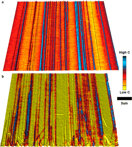
For this study, scientists grew a series of parallel nanotube lines, similar to the way nanotubes will be used in computer chips. Each nanotube was about 1 nanometer wide—ten times smaller than expected for use in the next generation of electronics. To explore the material’s properties, the researchers used microwave impedance microscopy (MIM) to image individual nanotubes.
“Although microwave near-field imaging offers an extremely versatile ‘nondestructive’ tool for characterizing materials, it is not an immediately obvious choice,” said Rotkin, a professor of physics and also of materials science and engineering. “Indeed, the wavelength of the radiation used in the experiment was even longer than what is typically used in optical microscopy—about 12 inches, which is approximately 100,000,000 times larger than the nanotubes we measured.”
He added: “The nanotube, in this case, is like a very bright needle in a very large haystack.”
The imaging method the researchers developed shows exactly where the nanotubes are on the silicon chip. More importantly, the information delivered by the microwave signal from individual nanotubes revealed which nanotubes were and were not able to conduct electric current. Unexpectedly, the researchers were finally able to measure the nanotube quantum capacitance—a very unique property of an object from the nano-world—under these experimental conditions.
“We began our collaboration seeking to understand the images taken by the microwave microscopy and ended by unveiling the nanotube’s quantum behavior, which can now be measured with atomistic resolution,” said Rotkin.
As an inspection tool or metrology technique, this approach could have a tremendous impact on future technologies, allowing optimization of processing strategies including scalable enriched nanotube growth, post-growth purification, and fabrication of better device contacts. One can now distinguish, in one simple step, between semiconductor nanotubes that are useful for electronics and metallic ones that can cause a computer to failure. Moreover this set of imaging modes sheds light on the quantum properties of these 1D structures.
Story by Lori Friedman
Posted on:


