Physicists map the strain in a wonder material

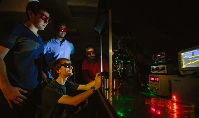
Slava V. Rotkin, professor of physics and of materials science and engineering, is working with an international research group to study the properties of graphene using spectroscopy and statistical analysis.
Graphene is the thinnest material known to science, and one of the strongest as well. A 1-atom-thick sheet of carbon, graphene was the first 2-dimensional material ever discovered. By weight, it is 150 to 200 times stronger than steel. It is also flexible, dense, virtually transparent and a superb conductor of heat and electricity.
In 2010, Andre Geim and Konstantin Novoselov won the Nobel Prize in Physics for their innovative experiments with graphene. Using ordinary adhesive tape, the two British physicists succeeded in peeling layers of graphene from graphite—no easy task considering that 1 millimeter of graphite consists of 3 million layers of graphene.
This week, an international group of scientists is reporting a breakthrough in the effort to characterize the properties of graphene noninvasively while acquiring information about its response to structural strain.
Using Raman spectroscopy and statistical analysis, the group succeeded in taking nanoscale measurements of the strain present at each pixel on the material’s surface. The researchers also obtained a high-resolution view of the chemical properties of the graphene surface.
The results, says Slava V. Rotkin, professor of physics and also of materials science and engineering, could potentially enable scientists to monitor levels of strain quickly and accurately as graphene is being fabricated. This in turn could help prevent the formation of defects that are caused by strain.
“Scientists already knew that Raman spectroscopy could obtain implicitly useful information about strain in graphene,” says Rotkin. “We showed explicitly that you can map the strain and gather information about its effects.
“Moreover, using statistical analysis, we showed that it is possible to learn more about the distribution of strain inside each pixel, how quickly the levels of strain are changing and the effect of this change on the electronic and elastic properties of the graphene.”
The group reported its results in Nature Communications in an article titled “Raman spectroscopy as probe of nanometer-scale strain variations in graphene.”
In addition to Rotkin, the article was authored by researchers from RWTH/Aachen University and the Jülich Research Centre in Germany; the Université Paris in France; Universidade Federal Fluminense in Brazil; and the National Institute for Materials Science in Japan.
In the decade or so since Geim and Novoselov began publishing the results of their research into graphene, the material has found its way into several applications, ranging from tennis rackets to smartphone touch screens. The 2013 market for graphene in the U.S., according to a 2014 article in Nature, was estimated at $12 million.
Several obstacles are holding up further commercialization of graphene. One of these is the presence of defects that impose strain on graphene’s lattice structure and adversely affects its electronic and optical properties. Related to this is the difficulty in producing high-quality graphene at low cost and in large quantities.
“Graphene is stable and flexible and can expand without breaking,” says Rotkin, who spent the fall of 2013 working at the RWTH/University of Aachen. “But it has wrinkles, or bubbles, on its surface, which give the surface a hilly feel and interfere with potential applications.”
A layer of graphene is typically made on a substrate of silicon dioxide by a process called chemical vapor deposition. The material can be strained by contamination that occurs during the process or because the graphene and the substrate have different thermal expansion coefficients and thus cool and shrink at different rates.
To determine the properties of graphene, the group used Raman spectroscopy, a powerful technique that collects light scattered off a material’s surface. The group also applied a magnetic field to gain additional information about the graphene. The magnetic field controls the behavior of the electrons in graphene, making it possible to see more clearly the effects of the Raman spectroscopy, Rotkin says.
“The Raman signal represents the ‘fingerprint’ of the graphene’s properties,” said Rotkin. “We’re trying to understand the influence of the magnetic field on the Raman signal. We varied the magnetic field and noticed that each Raman line in the graphene changed in response to these variations.”
The typical spatial resolution of the “Raman map” of graphene is about 500 nanometers (nm), or the width of the laser spot, the group reported in Nature Communications. This resolution makes it possible to measure variations in strain on a micrometer scale and determine the average amount of strain imposed on the graphene.
By performing a statistical analysis of the Raman signal, however, the group reported that it was able to measure the strain at each pixel and to map the strain, and the variations in strain, one pixel at a time.
Thus, the group reported, it was able to “distinguish between strain variations on a micrometer scale, which can be extracted from spatially resolved Raman maps, and nanometer-scale strain variations, which are on sub-spot-size length scales and cannot be directly observed by Raman imaging, but are considered as important sources of scattering for electronic transport.”
The group produced its graphene samples using chemical vapor deposition (CVD) at the RWTH/University of Aachen.
Rotkin and a dozen other researchers at Lehigh have submitted a CREF (Critical Research Equipment Fund) proposal to the university to purchase instrumentation to perform Raman mapping.
Rotkin supervises several graduate students in his lab and also includes undergraduate students from physics and other majors in his research.
Photos by Christa Neu
Posted on:


