Overlapping Opportunities

Tighter collaboration among researchers with Lehigh's Center for Photonics and Nanoelectronics, and its Center for Advanced Manterials and Nanotechnology, has potential impact upon a wide array of disciplines and application areas.
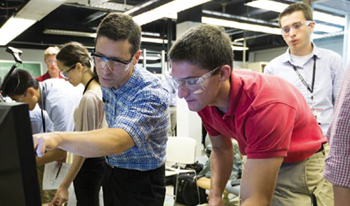
Rick Vinci (left) in Lehigh's Nano- and Micro-Mechanical Behavior Laboratory has been named director of the Center for Advanced Manterials and Nanotechnology.
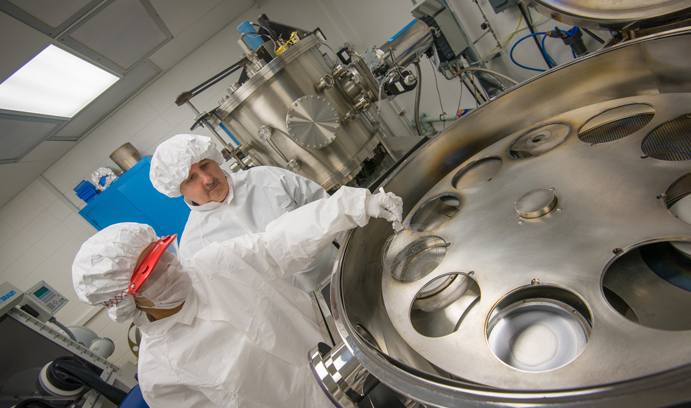
Graduate student Forough Mahmoudabadi works with Professor Miltos Hatalis to improve the performance of indium gallium zinc oxide transistors
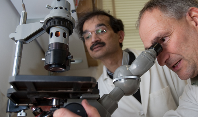
Prof. Himanshu Jain of materials science and engineering is part of a team funded by the NSF to create a new class of material called ferroelectric crystal-in-glass architecture, or FCGA, for next generation health and environmental monitoring devices, optical communications networks, consumer electronics, and more.
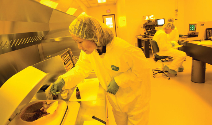
Lehigh's Center for Photonics and Nanoelectronics is a merger of two previous Lehigh research centers, the Center for Optical Technologies and the Sherman Fairchild Center for Solid State Studies. Nelson Tansu (see video link in column to right) was named CPN director upon its formation in the summer of 2014.
Where do great ideas originate?
From basic science that reveals new possibilities for applications? Or from an idea for a new technology that spurs the basic discoveries that need to be made?
One possibility: The best answer isn’t either/or but both/and. The most fruitful outcome incorporates both elements. Yet at many research institutions, the ingredients of innovation are separated: People in one area concentrate on fundamental science without thinking about how it might be used. People in another area imagine breakthrough applications before answering all the “how” questions.
Lehigh, however, has a long tradition of encouraging researchers to cooperate, says Richard Vinci, professor of materials science and engineering.
“We have many separate disciplines,” says Vinci, who directs the Center for Advanced Materials and Nanotechnology (CAMN), “but a surprising number of people, topics and research areas overlap.”
One major example of that cooperation is the collaboration between two research centers that both do much of their work at the nanoscale—CAMN and the Center for Photonics and Nanoelectronics (CPN).
If CAMN provides many of the fundamental discoveries that are developed into devices and other new technologies, CPN projects often begin with desired outcomes and work back toward the basic science necessary to bring a vision to life.
“CAMN tends to concentrate on fundamental materials opportunities,” Vinci says, “creating new materials and processes with new functionalities that can be plugged into new systems.”
CPN merges two previous centers, the Center for Optical Technologies, which was devoted to photonics research, and the Sherman Fairchild Center for Solid-State Studies, which concentrated on research in electronics and solid state devices.
“The goal of CPN,” says director Nelson Tansu, the Daniel E. (’39) and Patricia M. Smith Endowed Chair Professor in Photonics and Nanoelectronics, “is to transform the science of photonics and nanoelectronics in ways that help us develop material devices and device architecture to meet the grand challenges in society.
“By combining a strong foundation in computational, materials, devices and integrated systems with core expertise in photonics and nanoelectronics, we hope to enable CPN faculty and students to work on advancing the frontiers of science and technology with ambitious and long-term visions.”
Resources for innovation
Meeting the challenges of technological innovation now more than ever requires a meeting of minds from different fields. “The really interesting problems that can make a big impact tend to be beyond the ability of any one discipline to completely sort out,” Vinci says. “They require input from people with many different backgrounds.”
Collaboration broadens the pool of available expertise and introduces fresh thinking. “People who are not yet experts tend to ignore what seem to be obvious barriers to people who are experts,” Vinci says. “It turns out that a lot of those barriers aren’t real. If you don’t know they exist, you can accomplish things that surprise everybody.”
Cross-fertilization between CAMN and CPN has already taken place. “Even at the director level, Nelson and Rick have worked before on joint grants, so they know how that works and how everybody can benefit,” says Volkmar Dierolf, department chair and professor of physics within the College of Arts and Sciences. “There’s already quite a bit of overlap between CAMN and CPN, and a boost in the energy and resources invested in these centers will allow us to exploit their strengths even more.”
Both centers seek to leverage success in targeted areas where Lehigh has developed an international reputation—including characterizing properties at the nanoscale with electron microscopy, and analyzing and manipulating surfaces and interfaces.
“Being able to see things down to the nanometer or atomic scale allows you to understand materials at a level that’s really unprecedented,” Vinci says. “We have some of the best tools in the world at Lehigh for accomplishing that.”
Facilities available to the two centers include CPN’s Smith Family Laboratory for Optical Technologies, with material epitaxy and nanofabrication capabilities, a suite of electron microscopes in CAMN’s Nanocharacterization Laboratory, and Lehigh’s surface analysis facilities.
Among the powerful tools that these facilities house are spectroscopy instruments such as the high resolution x-ray photoelectron spectrometer (HR-XPS) and high-sensitivity, low-energy ion-scattering spectrometer (HS-LEIS), which provide extremely precise, high-resolution views of surfaces and subsurfaces that govern a material’s properties. World-class electron microscopes such as the JEM-ARM200F allow researchers to observe the chemical structure of a material at the atomic level, with specimens often prepared using a recently acquired FEI Scios DualBeam focused ion beam/scanning electron microscope. An array of instruments also allows researchers to optimize the growth of semiconductor materials on a variety of substrates.
With the help of such resources, “technology is evolving rapidly at what’s called the cyber-physical interface,” Tansu says. “In the past, the computing and physical worlds have largely been separate domains. We want to be able to transform the physical world and relate it to the cyberworld.”
To do that, says Tansu, CPN is also forming collaborations with researchers from Lehigh’s Environmental Initiative, Emulsion Polymers Institute and Integrated Networks for Electricity research cluster, and from academic departments in the sciences and engineering.
Two major thrusts
CPN’s goal is to channel Lehigh’s intellectual and physical resources in materials science, photonics and nanoelectronics into two key areas. The first is energy, sustainability and the environment, and the second is health, bioengineering and medicine.
In both areas, more advanced understanding of how photons, electrons and heat interact could lead to a wide variety of applications. These include making semiconductor-based lighting more efficient, enhancing energy storage in batteries, generating and storing solar energy, reducing industrial emissions, creating new materials that can be implanted in living tissue and even linking the mind to the body.
“Think of chronic pain relief,” Tansu says. It’s often treated with chemicals such as acetaminophen, ibuprofen or opioids, which can cause side effects, become addictive or lose effectiveness. “But if you understand electronics, photonics and biomaterials, you may be able to implant a very tiny integrated circuit in the body that releases heat directly to the point of pain when you need it and in the right amount.”
Implantable devices have already been used in microelectromechanical systems to replace joints and release glucose into the blood. Brain implants, or microchips on the surface of the skull that could detect, measure and control brain signals, represent a new frontier. “A chip implanted in the brain could control a lot of functionality,” Tansu says. “Integrating photonics and nanoelectronics, along with understanding biocompatible materials, requires researchers from CPN, CAMN and bioengineering.”
Similarly, developing the cyber-physical interface could not only make lights, solar panels and insulation more energy efficient, but also lead to smart-room technology in which your mere presence in a space triggers changes in its environment. Today, lights go on when you enter a room. “In the future, a room will recognize your preferences,” Tansu says. “It will know that at 7 a.m. you want a bright white light to help you start to be productive, and that by 3 p.m. you want a warmer tone.” If your spouse walks in, the room would know what to do when the two of you are present at the same time. Going a step further, if you look at curtains and imagine them closing, the curtains will close on their own.
Aside from incremental improvements in windows, structural materials and lighting, housing today is much the same as it was 50 years ago, Tansu says. “As we look to the future of sustainable living, we have to ask, ‘Can we design smarter, more energy-efficient living spaces that are based on viable modern technologies and not on past technologies?”
Greater efficiency in LEDs…
One area of sustainable living in which Lehigh already has contributed significant innovations—generating patents and winning interest from industry—is light-emitting diode (LED) technology. “Lehigh’s LED --work provides good examples of how teams working in collaboration can produce achievements that they wouldn’t have the expertise to accomplish alone,” Vinci says.
In one project, researchers simplified the growing of high-quality gallium nitride (GaN) on sapphire surfaces—a key to how much light an LED can generate.
A CAMN team including Vinci, Ph.D. student Jeffrey Biser and Helen Chan, department chair of materials science and engineering, created nanoscale patterns on a sapphire substrate to give its surface a variety of tiny topographical features. Tansu and Yik-Khoon Ee ’09 Ph.D. investigated the effect of the features on the growth of GaN. Together, the teams developed a growth method that took less time, cost less money, boosted quality, enhanced efficiency and resulted in a patent.
In a similar project, Tansu, Dierolf, Hongping Zhao ’10 Ph.D., Guangyu Liu ’14 Ph.D., Jing Zhang ’14 Ph.D. and Jonathan D. Poplawsky ’10 Ph.D. described approaches for optimizing the internal quantum efficiency for green light produced with indium gallium nitride.
“Currently, the green LEDs you find in stores are really blue LEDs that convert light to the rest of the visible spectrum,” says Dierolf. “It would be better to have the semiconductor itself emit green light. Our paper was significant because it showed a smart way to improve the efficiency of that color in the future of LED lighting.” Published in 2011 in Optics Express, the group’s paper ranked fifth in a ScienceWatch top 10 list of “What’s Hot in Physics” in January 2014.
Dierolf also has an NSF grant to try to reduce the size of lithium niobate and other crystalline materials that are used in the optical applications and modulators that drive the Internet. “It’s an advantage to confine light in smaller dimensions,” he says, “so devices and applications can use less space and material.”
Meanwhile, Dierolf and Prof. Himanshu Jain (materials science and engineering), have NSF funding to create a new class of material called ferroelectric crystal-in-glass architecture (FCGA).
“Making glass and doing it in bulk is fairly easy compared to making crystal, which is more delicate,” Dierolf says. “But crystals have better performance and specific functionalities.” Highly controlled short pulses from a femtosecond laser can reconfigure atomic structures to form crystals inside of glass. The process promises to combine the exceptional properties of crystal with the relative flexibility and low cost of glass—vital for the next generation of health and environmental monitoring devices, optical communications networks and consumer electronics.
… And energy and separations
Greater efficiency usually results in energy savings. Israel E. Wachs, the G. Whitney Snyder Professor of Chemical and Biomolecular Engineering, is developing new ways to convert natural gas efficiently into a liquid form that can be transported. This has major ramifications for an industry in which gas extracted at remote sites is often vented or flared, leading to environmental degradation and waste of resources. In another project, Wachs is looking to better understand the catalytic process by which biomass is converted to a renewable fuel.
Reducing emissions contributes to sustainable living as well. Research by Prof. Kai Landskron (chemistry, College of Arts and Sciences) shows that mesoporous material punctuated with nanoscale pores can electrically separate gases such as nitrogen and carbon dioxide. As he and colleagues write in Nature Communications, this may offer a low-cost method of reducing greenhouse gases from power plants.
“We want to understand the parameters that influence the size of the effect, its kinetics and whether the effect extends to other gases,” Landskron says.
Making materials porous usually makes them weaker, but mesoporous diamonds retain much of their inherent strength even under high pressure. That has implications for filtration membranes, nanooptics and drug delivery. “Diamonds are known to be biocompatible,” Landskron says. “It may be possible to load a drug into mesoporous diamond and release it in the body with less toxicity than with nanoporous silica.”
Broad applications could come from other NSF-funded efforts to better understand how material, biological and computational components interface with each other.
Research led by Profs. Filbert Bartoli (electrical and computer engineering), Xuanhong Cheng (materials science and engineering) and Sabrina Jedlicka (materials science and engineering) promises to push the frontiers of optical sensing, nanoplasmonics, biointerface design, nanofabrication, microfluidics, cell-based tissue and lab-on-a-chip technology. They're working to develop real-time sensing capabilities that would help differentiate and control the development of precursor cells that could be used in tissue transplantation—a major challenge in biomedicine.
Prof. Slava V. Rotkin (physics) is exploring a new class of rare-earth-based biocompatible materials in which nanoscale carbon tubes wrapped in DNA may acquire optical sensing capabilities.
"By learning the fundamental physics of nanoscale systems," says Rotkin, "we are not only engineering new devices and materials but establishing the foundations of theory as well." Rotkin recently spent a year abroad, working on graphene materials with physicists from RWTH Aachen University in Germany and with engineers from Sungkyunkwan University in Seoul, South Korea.
On the computational front, Prof. Heather Jaeger (chemistry) applies quantum mechanics equations to computer models that illuminate the sometimes-unexpected behavior of phenomena at the nanoscale. "Part of our job is helping to explain or provide a rationale for what happens in the lab by computing the properties that people are observing," Jaeger says.
Computation can also pave the way for discovery. By developing simulations of electron density in real time, Jaeger explores how negatively charged electrons and positively charged holes spatially separate when light or energy is applied. "Solar cell efficiency is based partly on charge separation, so we're exploring ways to do that better and better," Jaeger says. "To control electron and hole distributions, you need to understand what the driving forces are, and that's where our simulations come in."
Throughout CAMN and CPN, there's a push to integrate simulations and modeling into design and engineering in a movement called Integrated Computational Materials Engineering (ICME). "The goal is to enable the optimization of materials, manufacturing processes and component design, long before components are fabricated, by integrating the computational processes involved into a holistic system," says Prof. Natasha Vermaak (mechanical engineering and mechanics). "In the past, those have largely proceeded independently of each other."
Vermaak applies advanced optimization algorithms to thermostructural component design. The intent is to realize greater efficiency by optimizing material properties, fabrication processes, decision-making and, ultimately, the performance of new technologies.
This, in a nutshell, is the overarching aim of the two research centers.
"Our hope," says Vinci, "is to achieve even greater synergy by continuing to coordinate our activities and work together."
"With careful investment and coherent integration of the core expertise in the activities of our centers," says Tansu, "we believe our innovations can impact society for the next 15 to 20 years."
Posted on:

